


R.E.News future Technology-MIT combats e-waste with new Substrate Material for Flexible Electronics
 13/08/24-FR-English-NL-footer
Le MIT lutte contre les déchets électroniques grâce à un nouveau matériau de substrat pour l'électronique flexible
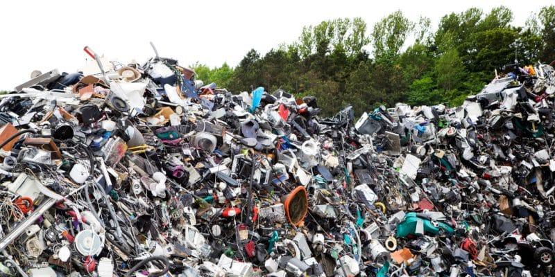 Image-FFr
Les déchets électroniques, ou déchets électroniques, constituent un problème mondial en pleine croissance, et il devrait s'aggraver avec la production de nouveaux types d'électronique flexible pour la robotique, les appareils portables, les moniteurs de santé et d'autres nouvelles applications, y compris les appareils à usage unique.
Un nouveau type de matériau de substrat flexible développé au MIT, à l'Université de l'Utah et à Meta a le potentiel de permettre non seulement le recyclage des matériaux et des composants à la fin de la vie utile d'un appareil, mais aussi la fabrication évolutive de circuits multicouches plus complexes que ceux fournis par les substrats existants.
Le développement de ce nouveau matériau est décrit cette semaine dans la revue RSC: Applied Polymers, dans un article du professeur Thomas J. Wallin du MIT, du professeur Chen Wang de l'Université de l'Utah et de sept autres personnes.
« Nous reconnaissons que les déchets électroniques constituent une crise mondiale permanente qui ne fera que s’aggraver à mesure que nous continuons à fabriquer davantage d’appareils pour l’Internet des objets et que le reste du monde se développe », explique Wallin, professeur adjoint au département de science et d’ingénierie des matériaux du MIT. À ce jour, de nombreuses recherches universitaires sur ce front ont visé à développer des alternatives aux substrats conventionnels pour l’électronique flexible, qui utilisent principalement un polymère appelé Kapton, un nom commercial pour le polyimide.
La plupart de ces recherches se sont concentrées sur des matériaux polymères entièrement différents, mais « cela ignore vraiment l’aspect commercial de la question, à savoir pourquoi les gens ont choisi ces matériaux au départ », explique Wallin. Le Kapton présente de nombreux avantages, notamment d’excellentes propriétés thermiques et isolantes et une disponibilité immédiate des matériaux sources.
Le marché du polyimide devrait représenter un marché mondial de 4 milliards de dollars d’ici 2030. « On le trouve partout, dans tous les appareils électroniques en gros », y compris dans des pièces telles que les câbles flexibles qui interconnectent différents composants à l’intérieur de votre téléphone portable ou de votre ordinateur portable, explique Wang. Il est également largement utilisé dans les applications aérospatiales en raison de sa grande tolérance à la chaleur. « C’est un matériau classique, mais il n’a pas été mis à jour depuis trois ou quatre décennies », explique-t-il.
Cependant, il est également pratiquement impossible de faire fondre ou de dissoudre le Kapton, il ne peut donc pas être retraité. Les mêmes propriétés rendent également plus difficile la fabrication de circuits dans des architectures avancées, telles que l’électronique multicouche. La méthode traditionnelle de fabrication du Kapton consiste à chauffer le matériau à une température comprise entre 200 et 300 degrés Celsius. « C’est un processus plutôt lent. Cela prend des heures », explique Wang.
Le matériau alternatif que l’équipe a développé, qui est lui-même une forme de polyimide et devrait donc être facilement compatible avec l’infrastructure de fabrication existante, est un polymère photopolymérisable similaire à ceux utilisés aujourd’hui par les dentistes pour créer des obturations résistantes et durables qui durcissent en quelques secondes avec la lumière ultraviolette. Non seulement cette méthode de durcissement du matériau est relativement rapide, mais elle peut fonctionner à température ambiante.
Le nouveau matériau pourrait servir de substrat pour des circuits multicouches, ce qui permet d’augmenter considérablement le nombre de composants pouvant être intégrés dans un petit format. Auparavant, comme le substrat Kapton ne fondait pas facilement, les couches devaient être collées ensemble, ce qui ajoutait des étapes et des coûts au processus. Le fait que le nouveau matériau puisse être traité à basse température tout en durcissant très rapidement à la demande pourrait ouvrir des possibilités pour de nouveaux dispositifs multicouches, explique Wang.
En ce qui concerne la recyclabilité, l’équipe a introduit des sous-unités dans le squelette du polymère qui peuvent être rapidement dissoutes par une solution d’alcool et de catalyseur. Ensuite, les métaux précieux utilisés dans les circuits, ainsi que des micropuces entières, peuvent être récupérés à partir de la solution et réutilisés pour de nouveaux appareils.
« Nous avons conçu le polymère avec des groupes esters dans le squelette », contrairement au Kapton traditionnel, explique Wang. Ces groupes esters peuvent être facilement brisés par une solution assez douce qui élimine le substrat tout en laissant le reste de l’appareil intact. Wang note que l’équipe de l’Université de l’Utah a cofondé une entreprise pour commercialiser la technologie.
« Nous décomposons le polymère en ses petites molécules d’origine. Nous pouvons ensuite récupérer les composants électroniques coûteux et les réutiliser », ajoute Wallin. « Nous savons tous que la chaîne d’approvisionnement est en pénurie pour les puces et certains matériaux. Les minéraux de terres rares qui entrent dans la composition de ces composants sont très précieux. Nous pensons donc qu’il existe désormais un énorme intérêt économique, ainsi qu’environnemental, à mettre en place ces processus de récupération de ces composants. »
L’équipe de recherche comprenait Caleb Reese et Grant Musgrave de l’Université de l’Utah, ainsi que Jenn Wong, Wenyang Pan, John Uehlin, Mason Zadan et Omar Awartani des Reality Labs de Meta à Redmond, Washington. Les travaux ont été soutenus par un fonds de démarrage du Price College of Engineering de l’Université de l’Utah.
NJC.© Info MIT
------------------------------------------------------------------------------------------------------------------
13/08/24-English
MIT combats e-waste with new Substrate Material for Flexible Electronics
Image-FFr
Electronic waste, or e-waste, is a rapidly growing global problem, and it’s expected to worsen with the production of new kinds of flexible electronics for robotics, wearable devices, health monitors, and other new applications, including single-use devices.
A new kind of flexible substrate material developed at MIT, the University of Utah, and Meta has the potential to enable not only the recycling of materials and components at the end of a device’s useful life, but also the scalable manufacture of more complex multilayered circuits than existing substrates provide.
The development of this new material is described this week in the journal RSC: Applied Polymers, in a paper by MIT Professor Thomas J. Wallin, University of Utah Professor Chen Wang, and seven others.
“We recognize that electronic waste is an ongoing global crisis that’s only going to get worse as we continue to build more devices for the internet of things, and as the rest of the world develops,” says Wallin, an assistant professor in MIT’s Department of Materials Science and Engineering. To date, much academic research on this front has aimed at developing alternatives to conventional substrates for flexible electronics, which primarily use a polymer called Kapton, a trade name for polyimide.
Most such research has focused on entirely different polymer materials, but “that really ignores the commercial side of it, as to why people chose the materials they did to begin with,” Wallin says. Kapton has many advantages, including excellent thermal and insulating properties and ready availability of source materials.
The polyimide business is projected to be a $4 billion global market by 2030. “It’s everywhere, in every electronic device basically,” including parts such as the flexible cables that interconnect different components inside your cellphone or laptop, Wang explains. It’s also widely used in aerospace applications because of its high heat tolerance. “It’s a classic material, but it has not been updated for three or four decades,” he says.
However, it’s also virtually impossible to melt or dissolve Kapton, so it can’t be reprocessed. The same properties also make it harder to manufacture the circuits into advanced architectures, such as multilayered electronics. The traditional way of making Kapton involves heating the material to anywhere from 200 to 300 degrees Celsius. “It’s a rather slow process. It takes hours,” Wang says.
The alternative material that the team developed, which is itself a form of polyimide and therefore should be easily compatible with existing manufacturing infrastructure, is a light-cured polymer similar to those now used by dentists to create tough, durable fillings that cure in a few seconds with ultraviolet light. Not only is this method of hardening the material comparatively fast, it can operate at room temperature.
The new material could serve as the substrate for multilayered circuits, which provides a way of greatly increasing the number of components that can be packed into a small form factor. Previously, since the Kapton substrate doesn’t melt easily, the layers had to be glued together, which adds steps and costs to the process. The fact that the new material can be processed at low-temperature while also hardening very quickly on demand could open up possibilities for new multilayer devices, Wang says.
As for recyclability, the team introduced subunits into the polymer backbone that can be rapidly dissolved away by an alcohol and catalyst solution. Then, precious metals used in the circuits, as well as entire microchips, can be recovered from the solution and reused for new devices.
“We designed the polymer with ester groups in the backbone,” unlike traditional Kapton, Wang explains. These ester groups can be easily broken apart by a fairly mild solution that removes the substrate while leaving the rest of the device unharmed. Wang notes that the University of Utah team has co-founded a company to commercialize the technology.
“We break the polymer back into its original small molecules. Then we can collect the expensive electronic components and reuse them,” Wallin adds. “We all know about the supply chain shortage with chips and some materials. The rare earth minerals that are in those components are highly valuable. And so we think that there’s a huge economic incentive now, as well as an environmental one, to make these processes for the recapture of these components.”
The research team included Caleb Reese and Grant Musgrave at the University of Utah, and Jenn Wong, Wenyang Pan, John Uehlin, Mason Zadan and Omar Awartani at Meta’s Reality Labs in Redmond, Washington. The work was supported by a start-up fund at the Price College of Engineering at the University of Utah.
NJC.© Info MIT
-----------------------------------------------------------------------------------------------------------------
13/08/24-NL
MIT bestrijdt e-waste met nieuw substraatmateriaal voor flexibele elektronica
Image-FFr
Elektronisch afval, of e-waste, is een snelgroeiend wereldwijd probleem en het zal naar verwachting verergeren met de productie van nieuwe soorten flexibele elektronica voor robotica, draagbare apparaten, gezondheidsmonitoren en andere nieuwe toepassingen, waaronder apparaten voor eenmalig gebruik.
Een nieuw soort flexibel substraatmateriaal dat is ontwikkeld bij MIT, de University of Utah en Meta heeft het potentieel om niet alleen de recycling van materialen en componenten aan het einde van de levensduur van een apparaat mogelijk te maken, maar ook de schaalbare productie van complexere gelaagde circuits dan bestaande substraten bieden.
De ontwikkeling van dit nieuwe materiaal wordt deze week beschreven in het tijdschrift RSC: Applied Polymers, in een artikel van MIT-professor Thomas J. Wallin, professor Chen Wang van de University of Utah en zeven anderen.
"We erkennen dat elektronisch afval een voortdurende wereldwijde crisis is die alleen maar erger zal worden naarmate we meer apparaten voor het internet der dingen blijven bouwen en naarmate de rest van de wereld zich ontwikkelt", zegt Wallin, universitair docent aan de afdeling Material Science and Engineering van MIT. Tot op heden is veel academisch onderzoek op dit gebied gericht op het ontwikkelen van alternatieven voor conventionele substraten voor flexibele elektronica, die voornamelijk een polymeer genaamd Kapton gebruiken, een handelsnaam voor polyimide.
Het meeste van dit soort onderzoek is gericht op compleet andere polymeermaterialen, maar "dat negeert echt de commerciële kant ervan, namelijk waarom mensen in eerste instantie voor de materialen kozen die ze hebben gekozen", zegt Wallin. Kapton heeft veel voordelen, waaronder uitstekende thermische en isolerende eigenschappen en een gemakkelijke beschikbaarheid van bronmaterialen.
De polyimide-industrie zal naar verwachting in 2030 een wereldwijde markt van $ 4 miljard zijn. "Het is overal, in feite in elk elektronisch apparaat", inclusief onderdelen zoals de flexibele kabels die verschillende componenten in uw mobiele telefoon of laptop met elkaar verbinden, legt Wang uit. Het wordt ook veel gebruikt in lucht- en ruimtevaarttoepassingen vanwege de hoge hittebestendigheid. "Het is een klassiek materiaal, maar het is al drie of vier decennia niet meer bijgewerkt", zegt hij.
Het is echter ook vrijwel onmogelijk om Kapton te smelten of op te lossen, dus het kan niet opnieuw worden verwerkt. Dezelfde eigenschappen maken het ook moeilijker om de circuits te produceren in geavanceerde architecturen, zoals gelaagde elektronica. De traditionele manier om Kapton te maken, omvat het verwarmen van het materiaal tot ergens tussen de 200 en 300 graden Celsius. "Het is een vrij langzaam proces. Het duurt uren", zegt Wang.
Het alternatieve materiaal dat het team ontwikkelde, dat zelf een vorm van polyimide is en daarom gemakkelijk compatibel zou moeten zijn met bestaande productie-infrastructuur, is een lichtuithardend polymeer dat vergelijkbaar is met die welke nu door tandartsen worden gebruikt om sterke, duurzame vullingen te maken die in een paar seconden uitharden met ultraviolet licht. Deze methode om het materiaal uit te harden is niet alleen relatief snel, het kan ook bij kamertemperatuur werken.
Het nieuwe materiaal zou kunnen dienen als substraat voor gelaagde circuits, wat een manier biedt om het aantal componenten dat in een kleine vormfactor kan worden verpakt, aanzienlijk te vergroten. Voorheen moesten de lagen aan elkaar worden gelijmd, omdat het Kapton-substraat niet gemakkelijk smelt, wat extra stappen en kosten aan het proces toevoegt. Het feit dat het nieuwe materiaal bij lage temperaturen kan worden verwerkt en tegelijkertijd zeer snel kan uitharden op aanvraag, zou mogelijkheden kunnen openen voor nieuwe meerlaagse apparaten, zegt Wang.
Wat betreft recyclebaarheid, introduceerde het team subeenheden in de polymeerruggengraat die snel kunnen worden opgelost door een alcohol- en katalysatoroplossing. Vervolgens kunnen edelmetalen die in de circuits worden gebruikt, evenals hele microchips, uit de oplossing worden gewonnen en hergebruikt voor nieuwe apparaten.
"We hebben het polymeer ontworpen met estergroepen in de ruggengraat", in tegenstelling tot traditionele Kapton, legt Wang uit. Deze estergroepen kunnen eenvoudig worden afgebroken door een vrij milde oplossing die het substraat verwijdert terwijl de rest van het apparaat ongedeerd blijft. Wang merkt op dat het team van de Universiteit van Utah een bedrijf heeft opgericht om de technologie te commercialiseren.
"We breken het polymeer terug in zijn oorspronkelijke kleine moleculen. Vervolgens kunnen we de dure elektronische componenten verzamelen en hergebruiken", voegt Wallin toe. “We weten allemaal van het tekort aan chips en sommige materialen in de toeleveringsketen. De zeldzame aardmineralen die in die componenten zitten, zijn zeer waardevol. En dus denken we dat er nu een enorme economische prikkel is, en ook een milieuprikkel, om deze processen te gebruiken voor het terugwinnen van deze componenten.”
Het onderzoeksteam bestond uit Caleb Reese en Grant Musgrave van de University of Utah, en Jenn Wong, Wenyang Pan, John Uehlin, Mason Zadan en Omar Awartani van Meta’s Reality Labs in Redmond, Washington. Het werk werd ondersteund door een startfonds van het Price College of Engineering van de University of Utah.
NJC.© Info MIT
------------------------------------------------------------------------------------------------------------------
Date de dernière mise à jour : 12/08/2024